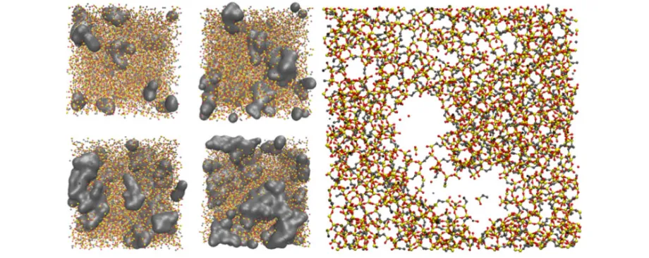
Image courtesy Dauskardt Group: In modeling new protective materials, the researchers introduced sacrificial molecules (shown in grey) in the four-frame simulation on the left. These molecules can be removed after the material is made, leaving behind tiny pores (visible in the larger frame on the right) that make the material more durable to expansion and contraction.
Stanford News - June 27th, 2016 - by Andrew Myers
Deep inside the electronic devices that proliferate in our world, from cell phones to solar cells, layer upon layer of almost unimaginably small transistors and delicate circuitry shuttle all-important electrons back and forth.
It is now possible to cram 6 million or more transistors into a single layer of these chips. Designers include layers of glassy materials between the electronics to insulate and protect these delicate components against the continual push and pull of heating and cooling that often causes them to fail.
A paper published today in the journal Nature Materials reshapes our understanding of the materials in those important protective layers. In the study, Stanford’s Reinhold Dauskardt, a professor of materials science and engineering, and doctoral candidate Joseph Burg reveal that those glassy materials respond very differently to compression than they do to the tension of bending and stretching. The findings overturn conventional understanding and could have a lasting impact on the structure and reliability of the myriad devices that people depend upon every day.
“It has always been assumed that these dense insulating materials react exactly the same way to being pushed as they do when pulled, as when they expand due to heat,” Dauskardt said. “We found that they are actually stiffer when compressed than when stretched, and we can use this knowledge to design more durable chips and devices.”
No perfect world
All electronic devices are in a constant state of flux, even those hanging on the wall or sitting on the desk. Imagine the stress upon a solar cell in the full sun of summer, or the continual calculations of the navigational app on your mobile phone. When active, the devices heat up and the components expand. When not in use, they cool and contract. This tug of war can destroy the device, Dauskardt said.
“We’re talking about a $250 billion industry that relies on these materials and which has always assumed that these push-pull properties were symmetrical. We now know that that’s not correct,” he added.
The materials’ response to this expansion and contraction is inherently related to the interaction within the network of particular atoms or groups of atoms – known as terminal groups – that do not fully bond during production.
In compression, these terminal groups strongly repel each other to make the network stiffer. In tension, like weak links in a chain, their failure to bond causes these very same atoms to interact less, making the materials less stiff and, consequently, to expand more than expected as they heat up.
“There’s no perfect world,” Dauskardt said. “If you could get rid of all of the unbonded terminal groups and create an absolutely flawless material, you would not see these asymmetries, but we can’t, so we have to understand and accommodate this knowledge in design.”
Surprising results
These previously unknown asymmetries will have fundamental implications on calibrating computer models used to craft new materials and electronic components. Materials scientists will now have to integrate these findings in their mathematical algorithms, which currently assume that the stiffness is symmetrical.
“This was a very surprising result. It’s not something that we would have expected and it has important implications for industry,” Dauskardt said.
Practically speaking, in the long run, this new knowledge could improve reliability and durability of electronic devices whose delicate circuits are compromised by the continual strains of everyday use.
The research was funded by the Department of Energy. The paper is titled “Elastic and Thermal Expansion Asymmetry in Dense Molecular Materials.”

